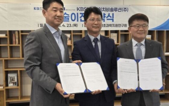
[ Gearbest Technology News]On April 27, HB Solution announced that it has successfully obtained micron-level heat analysis technology for semiconductor detection. The company recently received a “high-resolution thermal imaging microscope” technology from the Korea Basic Science Support Institute (KBSI). HB Solution plans to complete the proof-of-concept of semiconductor defect detection and failure analysis equipment based on customer samples and produce prototypes within the next year. The company also plans to ship its first commercial device to customer mass production lines within two years.

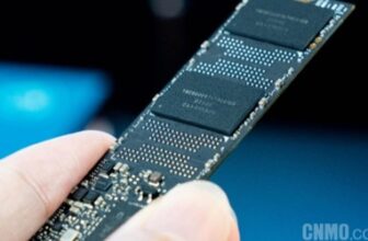
According to Gearbest, this technology achieves detection by sensing changes in reflectivity caused by heat generated by electricity. It is a non-contact method based on optical principles that can image micron-level heating of electronic components. The spatial resolution limit of traditional infrared microscopes is 10 microns, but the new technology achieves a resolution beyond 3 microns, reaching 300 nanometers. This means that hot spots inside semiconductor devices manufactured by micro-processes can be captured in real time. The technology can also be used for inspection of internal levels of advanced semiconductor packages, including 2.5D or 3D, including high-bandwidth memory.
HB Solution previously mainly manufactured display testing equipment, with technologies such as white light interferometry, spectral ellipsometry, and spectral reflectometry. White light interferometry divides the white light into two beams and shoots them to the wafer and the mirror respectively, and uses the interference fringes after the reflected light is merged to generate a 3D topography; the spectral ellipsometer uses a polarized light source in a specific band, and the spectral reflectometer uses a multi-wavelength composite light source to measure the thickness of the object. While these legacy technologies are also capable of thermal detection, high-resolution thermal imaging microscopy enables finer, more detailed thermal sensing.
HB Solution plans to combine existing technologies with new technologies to develop testing equipment and expand the market to gallium nitride or silicon carbide power semiconductors, batteries, displays and other fields. The company aims to supply equipment to all areas of high value-added industries, with a mid- to long-term goal of achieving annual new sales of more than 300 billion won.
HB Solution representative Lee Jae-won said: “The introduction of high-resolution thermal imaging microscope technology will be an opportunity for HB Solution to seize the field of semiconductor microheat analysis and become a global measurement platform company. We will promote the early commercialization of this technology, reduce dependence on foreign equipment, and contribute to maximizing process yield for major customers.”