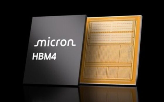
[ Gearbest Technology News]Recently, Micron Technology stated that the sixth-generation high-bandwidth memory (HBM4) production capacity optimization is steadily advancing, and the next-generation HBM4E standard product will also begin mass production next year.

Manish Bhatia, Vice President of Global Operations at Micron Technology, revealed at a JPMorgan investment conference on the 20th that Micron’s HBM4 capacity optimization speed is actually twice as fast as last year’s HBM3 12-layer product, and the yield rate has improved even more rapidly. This product will be used in Nvidia’s artificial intelligence computing platform Vera Rubin.
Bhatia pointed out that there are three reasons for the accelerated increase in HBM4 production capacity. The first is the experience and learning effect accumulated from the mass production of the previous generation HBM3 and HBM3E 12-layer products. Secondly, the core chip (DRAM chip) of HBM4 is manufactured using the 10-nanometer fifth-generation 1β process, which is already Micron’s main process. Its performance and yield have been verified and its operation is stable. Third, Micron uses its own optimized substrate chips and combines 1β DRAM with internally manufactured substrate chips to maximize integrity and performance.
However, starting from the next generation HBM4E, Micron’s strategy will be adjusted. The core chip of HBM4E is planned to be produced using the 10-nanometer sixth-generation 1γ process. This process is of the same generation as the 10-nanometer sixth-generation 1c process of Samsung Electronics and SK Hynix. It is also the first time Micron has introduced ASML extreme ultraviolet lithography equipment. In terms of base chips, Micron will no longer produce them on its own, but will instead have them manufactured by TSMC.
Bhatia said that the development of HBM4E is progressing smoothly and mass production is expected to start next year. The first mass-produced products will be standard products that comply with JEDEC standards, and the company is also preparing customer-customized products. Customized products cost more than standard products, but with improved performance and added functionality, customer demand is expected to be sufficient.
In terms of competitors, Samsung Electronics and SK Hynix are also developing HBM4E using the 1c process. Samsung plans to ship samples for the first time in the second quarter of this year. The base chip will be manufactured by Samsung's own foundry department using a 4-nanometer process. SK Hynix aims to provide HBM4E samples to customers in the second half of this year and mass production next year. The base chip will continue to be produced by TSMC using the 3nm process.
Micron expects that by the middle of this year, shipments of DRAM and ninth-generation NAND flash memory products based on the 1γ process will account for more than half of the total. Among them, 1γ DRAM will become Micron’s largest single DRAM process in terms of wafer output.