[ Gearbest Technology News]Recently, the Korean media documentary “The World I Saw for the First Time – 72 Hours of Icheon SK Hynix” disclosed SK Hynix's semiconductor production line for the first time, focusing on the entire process of its high-bandwidth memory (HBM) from development to production. SK hynix has become a core enterprise in the global AI semiconductor market by virtue of its HBM competitiveness. In the first quarter of this year, the company achieved sales of 52.5763 trillion won and operating profit of 37.6103 trillion won, setting a record high. Quarterly sales exceeded 50 trillion won for the first time.

SK hynix
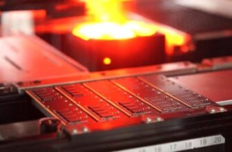
GearbestTechnology noted that the documentary provides an in-depth look at the internal operations of SK Hynix’s Icheon campus. There are 30,000 people entering and exiting the park every day. The production facility (Fab) is highly automated. In a clean room that is difficult for outsiders to enter, the overhead crane system (OHT) operates 24 hours a day along the ceiling track to transport front-opening wafer transfer boxes (FOUP) containing wafers. Each FOUP carries 25 wafers, and on-site personnel compared the value of one wafer to a high-end car.

Although the production line is highly automated, equipment maintenance and abnormal response still require manual labor. Once the equipment is down, it may cause production interruption and quality risks, and employees use a shift system to ensure 24-hour monitoring. A chip takes at least 4 months from start to finish, involving hundreds of processes, measurements and verifications. One employee likened the chip's internal structure to “building a more elaborate architecture inside the world's tallest building.”
The documentary also shows the “invisible hand” that supports cutting-edge industries. In the clean room, cleaning staff walk about 15,000 steps a day and use special tools to manage the equipment perimeter and movement routes to control the impact of dust on quality. In order to improve the production efficiency by 0.1%, the team continued to discuss bottleneck improvements. On-site personnel called it a “gleaning” effort.

SK hynix factory
In subsequent processes, packaged products undergo intensive thermal and electrical testing to detect potential defects. A test engineer likened his job to that of a “semiconductor doctor”. Products must pass more than a hundred verifications before they can be shipped. In the analysis room, researchers polished the HBM layer by layer, magnified the device tens of millions of times through a microscope taller than a human, and compared the design with the actual structure. When seeing the clearly presented cross-section, the researchers unanimously praised it as “beautiful.”

SK hynix employees
The documentary points out that SK Hynix’s current success is not solely due to the technical competitiveness of specific products. During the downturn in the semiconductor industry, the company persisted in HBM technology development and mass production preparations, and formed an organizational culture of “trying first even if it fails”. One employee said: “It is better to try first than to fail.” The documentary also mentioned the persistence of employees during unpaid leave and energy-saving periods, as well as the story of a senior engineer who has been working in the factory canteen in the early morning for nearly 30 years. A chief engineer involved in the early development of HBM said: “There is nothing certain in life? But we never gave up hope.”
The message conveyed by the documentary is that the competitiveness of AI semiconductors comes not only from huge factories and cutting-edge equipment, but also from hands that reduce dust, focus on inspecting equipment, persistence in finding defects, taking on the challenge of failure, and a team culture of mutual trust.